The PLL
The purpose of the PLL is to multiply the reference frequency up to 200MHz for the FPGA to use to generate the high speed counter. Anyone familiar with the Xilinx FPGAs might be wondering at this point why I’m not using the built-in Digital Clock Manager (DCM) on the Spartan 3. The blocker for that idea is that the DCM minimum clock input is 18MHz and in any case the output RMS jitter is rather high at around 250ps compared to approximately 1ps for the device used here.
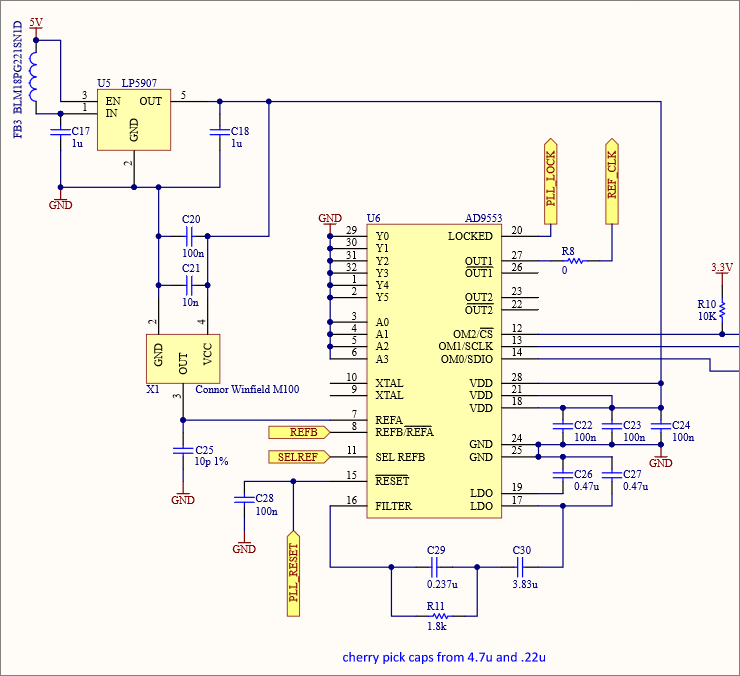
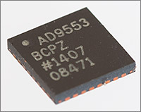
I’ve selected the Analog Devices AD9553 as the external PLL. It’s a very high quality, low jitter device available in an annoying QFN package.
The AD9553 is full of features and must be externally programmed over SPI before it’ll lock on and generate my target frequency frequency.
The Ax and Yx pins can be used by the AD9553 to hard-select from a range of predefined configurations and can be used as an alternative to SPI programming. Grounding all these pins selects SPI as the active configuration mode and gains access to far more options.
The AD9553 supports two separate inputs and has a pin to select between those. I use these to connect the onboard TCXO and the external reference input and use GPIO from the MCU to select between them.
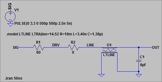
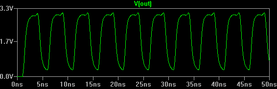
The 200MHz LVCMOS output is presented on pin 27. I placed a footprint on the board for a series termination resistor in case I need to suppress any ringing on the output. The best way to check if you’re going to have signal integrity issues on a high frequency line is to simulate it as a transmission line using the LTSPICE circuit simulator.