
The FPGA Design
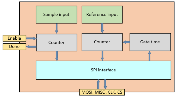
A block diagram of the FPGA design is shown above. It’s quite simple but does require some high speed processes. The flow of control works like this.
- The MCU programs a gate counter using the SPI interface.
- The FPGA receives a rising edge on its ‘enable’ input.
- Counting begins at the next rising edge of the sample input and ‘done’ goes low.
- When the reference counter reaches the gate limit counter then counting stops at the next rising edge of the sample clock.
- Done goes high.
- The MCU reads the two counters using the SPI interface.
It’s all quite straightforward and you can view the VHDL source code here on github. The important parts of the system are the 31-bit counters, and in particular the reference counter. These must be able to cope with counting at 200MHz. The choice of counter width is a trade off between counter speed and the maximum counter value. At 31 bits I can cope with up to 10 seconds of counting and hence the maximum gate time is 10 seconds.
A typical synchronous counter, of the type automatically created for you by the synthesiser when you use an addition-by-one expression, is not fast enough to count at 200MHz. To get to that sort of speed requires a faster implementation and I chose to reuse one available here at opencores.org.
The side effect of using a pipelined counter such as this is that counting takes more than one clock cycle. In this design that means that several clock cycles are used after the gate time has ended to flush the pipeline and let the counter settle. This can be seen in this ISIM simulation screenshot. Notice how the counters continue to update for a few clock cycles after the done_counting bit is set.
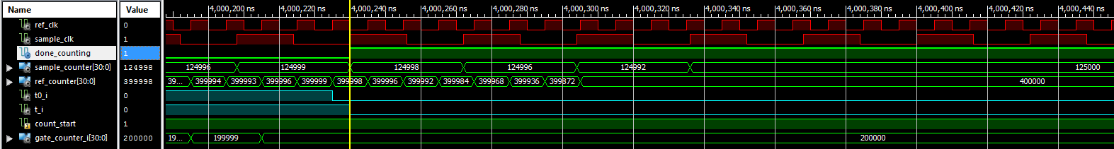
Pipelined counter operation (click for larger)
Xilinx ISIM… oh dear the bitrot really is starting to affect these venerable old tools. On Windows 7 ISIM was stable but clunky to use but now on Windows 10 it’s started to crash during certain common UI operations. Xilinx aren’t interested so it looks like the only solution if you need crash-free operation is to run Windows 7 in a VM.
To ensure that my timing goals are met I add timing constraints to the .ucf file:
TIMESPEC TS_ref_clk = PERIOD "ref_clk" 5 ns HIGH 50 %;

NET "inst_equal_precision_counter/ref_clk_div" TNM_NET = "inst_equal_precision_counter/ref_clk_div";
TIMESPEC TS_ref_clk_div = PERIOD "inst_equal_precision_counter/ref_clk_div" 10 ns HIGH 50 %;

NET "sample_clk" TNM_NET = "sample_clk";
TIMESPEC TS_sample_clk = PERIOD "sample_clk" 20 ns HIGH 50 %;

NET "spi_clk" TNM_NET = "spi_clk";
TIMESPEC TS_spi_clk = PERIOD "spi_clk" 20 ns HIGH 50 %;
Inspecting the verbose output from the post-PAR timing report shows whether I’ve managed to meet my timing constraints:
Timing constraint: TS_ref_clk = PERIOD TIMEGRP "ref_clk" 5 ns HIGH 50%;
For more information, see Period Analysis in the Timing Closure User Guide (UG612).

 120 paths analyzed, 120 endpoints analyzed, 0 failing endpoints
 0 timing errors detected. (0 setup errors, 0 hold errors, 0 component switching limit errors)
 Minimum period is   2.592ns.
All my constraints are met and this design can run well in excess of the 200MHz target. There’s no point in optimising any further once all constraints are met so it’s time to move on to the next part of the design.


