
Building the board
To build the board I followed my usual process of tinning the pads, applying flux and then balancing the components on the tinned pads. The board is then carefully placed in my reflow oven and I execute a ‘leaded’ reflow profile. At around 180°C the little bumps of solder melt and the components sit down onto the pads.
The QFN is of course the biggest unknown in the process because of the ground pad that’s completely hidden from view. The ground pad must be connected and it must also have multiple via connections to a solid plane. The trick is getting just enough solder so that it will sit down onto the board at the same level as the surrounding pads and the solder must not wick away down the vias leaving you with nothing left on top. Of course you can’t visually check that you’ve got it right after the reflow, nor can you touch it up if you get it wrong.
If the pad is the device’s only connection to ground then you can test its continuity by probing the little supporting spurs that are exposed at the end of the rows of pads. I really dislike the QFN package but they’re here to stay so developing a repeatable assembly process is really important.
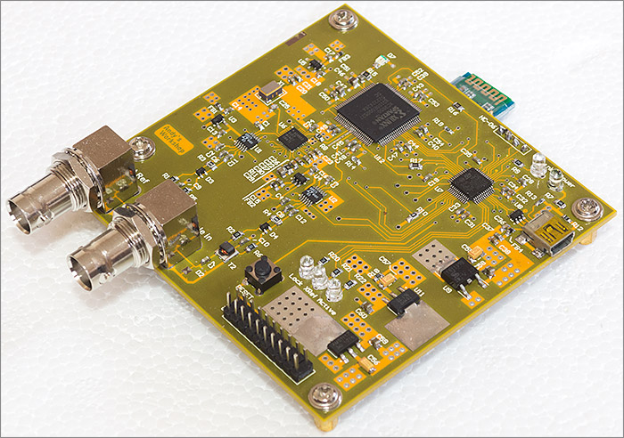
Here it is fully assembled and looking great in my opinion. I’ve opted to stick the HC-06 underneath the board with a double-sided sticky pad and connect it with wires to the 2.54mm header on the main board. It’s designed to stick out by about 20mm so that the bluetooth antenna is not obstructed.


