
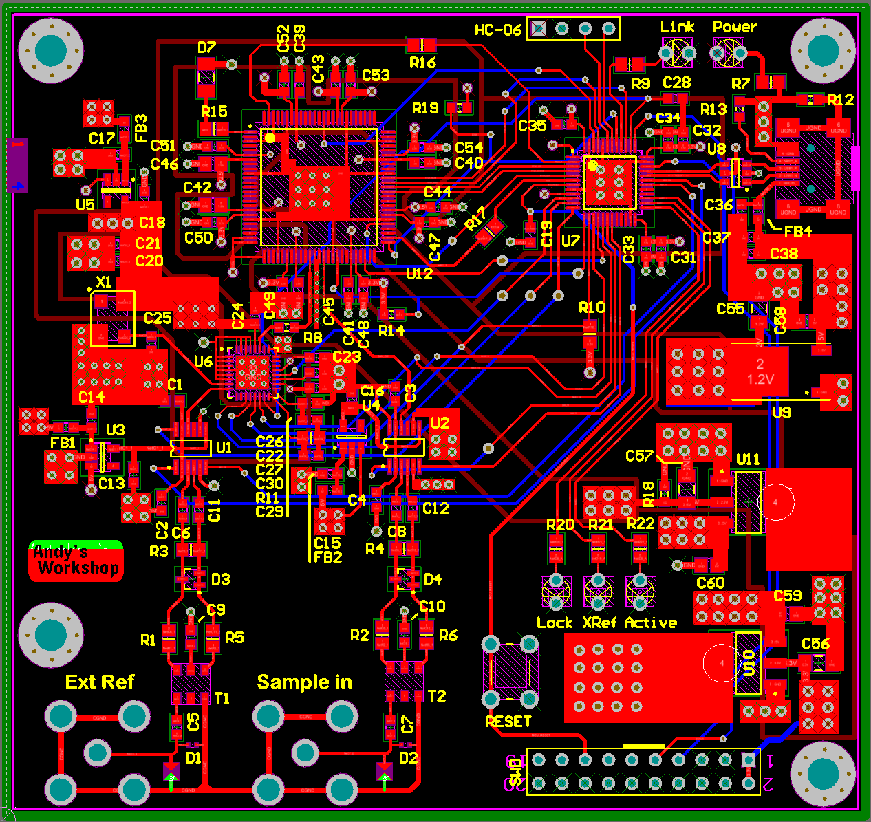
Board Layout
Now I’ve got a schematic that I’m happy with it’s time to consider the board layout. I’ve already decided that this is going to be a four layer board with a stackup that looks like this.
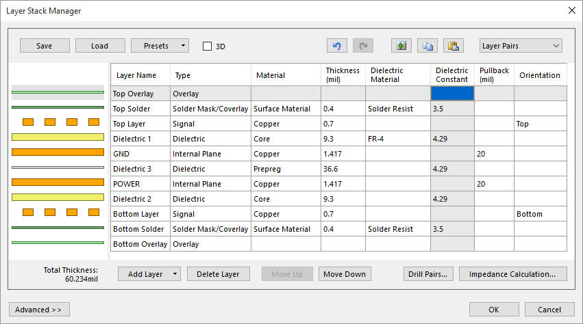
The main driver for choosing four layers instead of the cheaper two layers is that I’ve got both analog and high speed digital circuits on this board and I really want a continuous unbroken ground plane beneath the top signal layer to help with signal integrity and allow me to have controlled impedance traces. I’ll also benefit from simpler routing around the FPGA with the ability to run all those different power supplies through an inner plane.
Click for a larger image
I want to use the great value prototyping services from PCBWay, ITead, Seeed and others which means that I really need to keep the board size to 10x10cm because there’s a large price jump for four layer boards above that level.
Most of the signals, including all the 50Ω controlled impedance traces are on the top layer with the bottom layer used for additional routing. Large copper fills with multiple vias to the solid ground plane are located near to each of the sensitive components so that they have a low noise, low impedance path to ground.
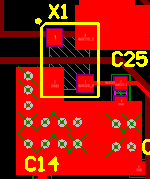
Local fill with multiple vias to ground
The digital components, primarily the FPGA and the MCU are located such that their return signals through the ground plane do not pass under the analog components. Furthermore, chassis ground for the BNC connectors is isolated from the PCB ground.
My previous FPGA design, the graphics accelerator, drew more current from the 3.3V supply than I was expecting, resulting in the AMS1117 regulator getting rather hot. I’ve learned my lesson from that and have included large exposed copper fills around the FPGA regulators that can be used to dissipate the heat throughout the PCB.
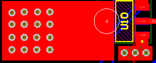
Large heatsink area for the AMS1117 is also mirrored on the bottom layer
The fill next to the AMS1117 is sized to accept one of those little RAM IC heatsinks that you can get on ebay. I don’t know if I’ll need one at this stage but there’s room for overkill on this board so better to be safe than sorry.

Layer stack telltale
Over on the left of the board you can see a row of numbers. This is a trick I use to make sure that the manufacturer gets the layer stackup correct. I include the numbers 1..4 sequentially in the copper on each layer from top to bottom and remove the solder mask from top and bottom and the copper from around the numbers so that I can see through the board when it’s held up to the light. If the manufacturer has got the inner layers the right way around then I’ll be able to view the 1..4 sequence with decreasing brightness from front to back.
I made a small mistake in my implementation of this feature in that I forgot to remove the copper from the inner layers surrounding the numbers. The feature still works though. If the manufacturing is correct then I will be able to see 1,2 when viewed from the top and 3,4 when viewed from the bottom.
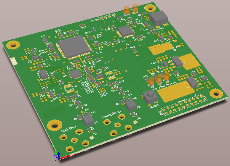
The 3D view of a board is not just for show, it’s really useful for checking to see if you’ve made common mistakes such as overlapping component labels or labels straying over vias or pads.


