
Function Set
Set the size of interface with the data bus (DL), number of lines in the LCD (N) and character type (F).
|
RS
|
R / W
|
DB7
|
DB6
|
DB5
|
DB4
|
DB3
|
DB2
|
DB1
|
DB0
|
|
0
|
0
|
0
|
0
|
1
|
DL
|
N
|
F
|
X
|
X
|
Set the CG RAM Address
The LCD module defined in addition to all the ASCII character set allows the user to define 4 or 8 characters. The composition of these characters is saved to a CG RAM memory called up to 64 bytes. Each user defined character consists of 16 or 8 bytes that are stored in successive positions of the CG RAM.
Using this instruction sets the CG RAM memory address from which the bytes will be stored that define a character. Running this command all the data that is subsequently read or write this memory made from CG RAM.
|
RS
|
R / W
|
DB7
|
DB6
|
DB5
|
DB4
|
DB3
|
DB2
|
DB1
|
DB0
|
|
0
|
0
|
0
|
1
|
CG RAM Address
|
|||||
Set the DD RAM Address
The characters or data to be displayed is stored in a memory called RAM DD then move on to the screen.
Using this instruction sets the address of DD RAM memory from which data will be stored to be displayed. Running this command all data being written to or read then they will from the DD RAM memory.
8Fh addresses 80h to 16 characters correspond to the first row and addresses C0h to CFH to 16 characters of the second row, for this model LCD.
|
RS
|
R / W
|
DB7
|
DB6
|
DB5
|
DB4
|
DB3
|
DB2
|
DB1
|
DB0
|
|
0
|
0
|
1
|
DD RAM Address
|
||||||
Read Busy Flag and Address
E l LCD module takes some time to execute instructions, at which time you should not send another instruction. This flag has a BUSY (busy) indicating that an instruction is being executed.
This reading instruction reports the status of the flag as well as providing the address counter value of the CG RAM or DD RAM according to the latest that has been used.
|
RS
|
R / W
|
DB7
|
DB6
|
DB5
|
DB4
|
DB3
|
DB2
|
DB1
|
DB0
|
|
0
|
1
|
BF
|
Address DD RAM or CG RAM
|
||||||
Write data to CG or DD RAM
Command to write to DD RAM memory the data to be presented on the screen in ASCII code.
Also written to CG RAM memory bytes to generate user-defined characters.
Previously DD RAM memory addresses or CG RAM memory where you want to write data.
|
RS
|
R / W
|
DB7
|
DB6
|
DB5
|
DB4
|
DB3
|
DB2
|
DB1
|
DB0
|
|
1
|
0
|
Byte ASCII character or graphic
|
|||||||
Read Data from CG RAM or DD RAM
Command to read data stored in DD RAM, ASCII code.
Likewise, read CG RAM memory bytes of user-defined characters.
Previously, memory addresses or memory DD RAM CG RAM you want to read the data.
|
RS
|
R / W
|
DB7
|
DB6
|
DB5
|
DB4
|
DB3
|
DB2
|
DB1
|
DB0
|
|
1
|
1
|
Byte ASCII character or graphic
|
|||||||
DOWNLOAD SOURCE CODE and Firmware
the Software is written with avr studio 5.0 and with AVR gcc GNU compiler
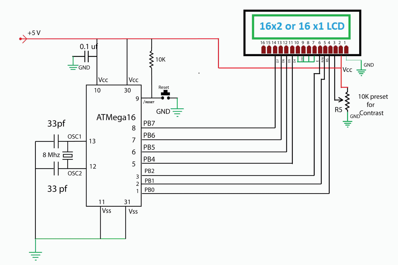
click here to download: —- 4 bit mode

Original Article by Gaurav Singh at Embedded Engineering.
[tps_footer][/tps_footer]
Pages: 1 2


