
I have built a little FPGA board Xilinx xc3s250e called WireFrame. the board is only 50mm x 25 mm in size and it is possible to breadboard it. board also has 32MByte SDRAM, 4MByte serial Flash for storage. total 3 2A max each Switching regulator for Vcc I/O 3.3V (adjustable trough regulator feed back resistors), VCCAUX 2.5 V and VCCINT 1.2v.
the first version of the board also had some switching boost circuit to generate various rails for E-ink displays. we don’t need this feature for our current project. actually a little while back , I was working on project which interface a 6” E-ink display to a ARM CPU Running Linux. the over all Requirement was in such shape it was not possible directly interface the display to the Linux machine because of the way raw e-ink screen works.E-ink screen does not have any intelligent controller built-in it has only a few Row and column driver which make the whole thing work. so I worked a little FPGA solution to work as controller instead going for standard controller IC because of few reasons.
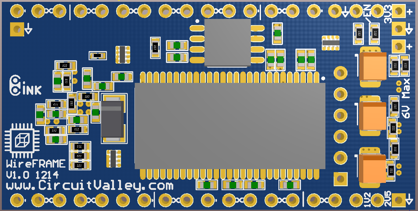
The FPGA Board

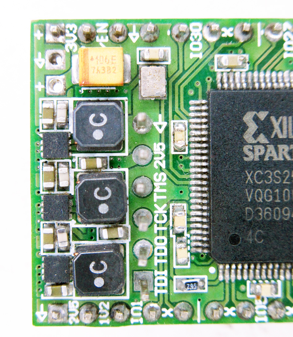
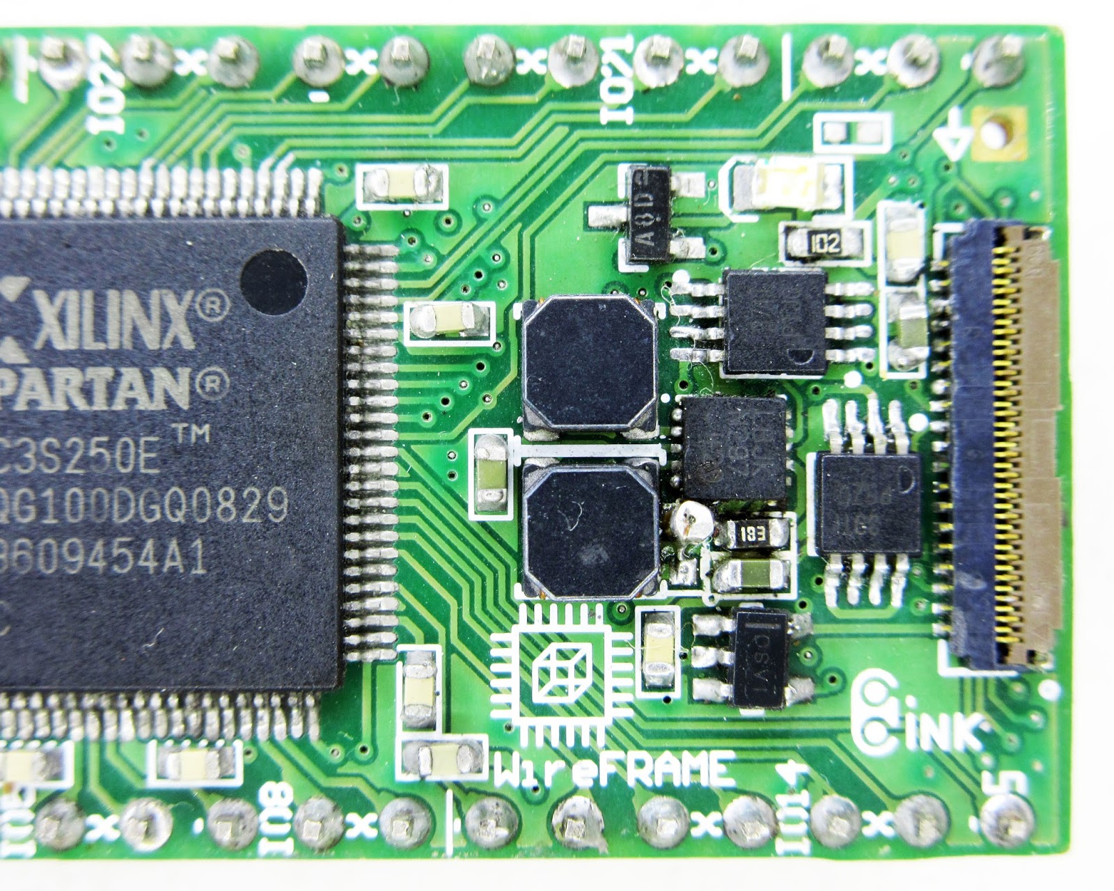
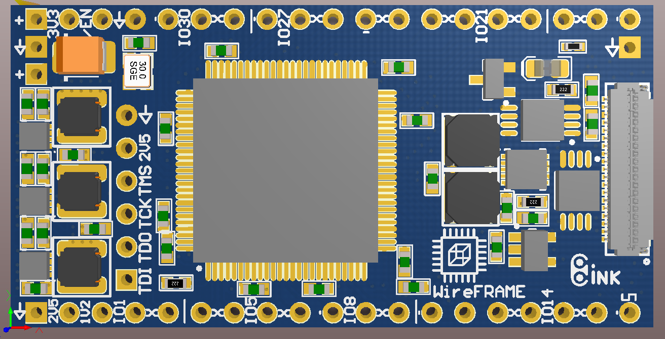
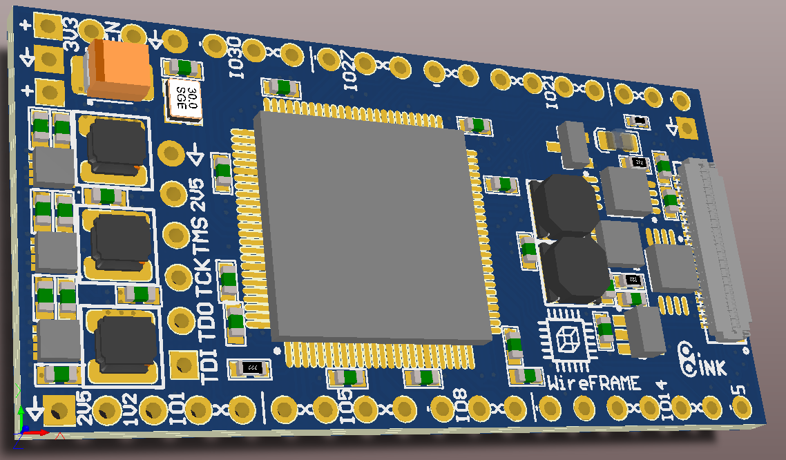
The board “WireFrame” has Xilinx XC3S250E at its core ,has 4MByte serial flash for bit-stream storage,32 MByte of SDRam and a small 25Mhz crystal oscillator (can be used FPGA’s DCMs to multiply the clock upto hundreds of Mhz), total 3 2A each power regulator with maximum 6V input ,one regulator each For VccI/O 3.3V , VccAUX 2.5V and VccINT 1.2V. board completely breadboard-able , has two 19pin 0.1” pitch header to be inserted into breadboard. out of total 19 pins there are power input , all 3 regulator’s output, FPGA reset and FPGA I/O them self , few I/O are marked with capability of being configurable as differential pair.a six pin 2.5V JTAG header is separate for FPGA bit-stream download. board comes in very small size of only 50x25mm.
PCB has 4 layers 2 for signal and 2 for power. PCB is designed with trial version of altium and source code gerber file are available for download form github repo https://github.com/circuitvalley/WireFrame-FPGA
The FPGA
the Xilinx XC3S250E it has 250K logic blocks 73Kbit Distributed RAM bits , 360K block ram , 20 Dedicated Multipliers , 4 DCMs. we have used VQG100 package which is very small for such a big FPGA for the shake of small board size. With VQG100 package we got only total 66 I/O (including input only) lines , 30 differential lines. more details how the FPGA is configured to boot ,powered and connected to other peripheral please refer to the schematic.
The DRAM
we have used winbond w9825g6 4 M x 4 BANKS x 16 BITS SDRAM.The RAM is mounted on the bottom side of the board ,it is in TSOP II 54-pin, 400 mil Package

The Serial Flash
we have used .
The Power regulators
we have used TPS62065QDSGRQ1 3Mhz 2A setpdown converter in a very small 2×2 SON package to keep the whole board profile as low as possible. Regulator take upto 6V inputs , same regulator is used to generate all 3 power rails in the system , each regulator can take upto 2A current , current consumption of the FPGA depends totally on the Design FPGA is running.
Downloading the Bit-stream
the board does not have any any programmer on board , it only expose a 6 pin header for JTAG based programming . you can use any xilinx programmer you like there are many programmer available other there. we are also planning to make programmer in future but for now you have to getaway with some third party programmer.
The Board Schematic

Expesion Header Pinout
Source and Gerber file
board is completely opesource and all the design file and gerber files are freely available in the github repo of circuitvalley
https://github.com/circuitvalley/WireFrame-FPGA
PCB 3D

 |
 |
![]()


