Understanding the register file
The register file is a key component of the ARM1, storing information inside the chip.
(As a RISC chip, the ARM1 makes heavy use of its registers.)
The register file consists of 25 registers, each holding 32 bits. This section describes step-by-step how the register file is built out of individual transistors.
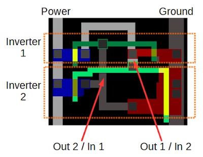
The diagram below shows two transistors forming an inverter. If the input is high (as below), the NMOS transistor (red) turns on, connecting ground to the output so the output is low. If the input is low, the PMOS transistor (blue) turns on, connecting power to the output so the output is high. Thus, the output is the opposite of the input, making an inverter.
Combining two inverters into a loop forms a simple storage circuit. If the first inverter outputs 1, the second inverter outputs 0, causing the first inverter to output 1, and the circuit is stable. Likewise, if the first inverter outputs 0, the second outputs 1, and the circuit is again stable. Thus, the circuit will remain in either state indefinitely, “remembering” one bit until forced into a different state.
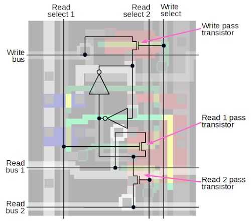
To make this circuit into a useful register cell, read and write bus lines are added, along with select lines to connect the cell to the bus lines.
When the write select line is activated, the pass connector connects the write bus to the inverter, allowing a new value to be overwrite the current bit.
Likewise, pass transistors connect the bit to a read bus when activated by the corresponding select line, allowing the stored value to be read out.
To create the register file, the register cell above is repeated 32 times vertically for each bit, and 25 times horizontally to form each register.
Each bit has three horizontal bus lines — the write bus and the two read buses — so there are 32 triples of bus lines. Each register has three vertical control lines — the write select line and two read select lines — so there are 25 triples of control lines. By activating the desired control lines, two registers can be read and one register can be written at a time.[11]
When the simulator is running, you can see the vertical control lines activated to select registers, and you can see the data bits flowing on the horizontal bus lines.
By looking at a memory cell in the simulator, you can see which inverter is on and determine if the bit is a 0 or a 1.
The diagram below shows a few register bits. If the upper inverter input is active, the bit is 0; if the lower inverter input is active, the bit is 1.
(Look at the green lines above or below the bit values.) Thus, you can read register values right out of the simulator if you look closely.


