
While most of my microcontroller designs run on 3.3 volts there is still the ocasional 5 volt design. Or I do something with an Arduino. So the need may arise to interface between logic working at different voltage levels. There are several ways of doing this, depending on your needs. Things are relatively simple as long as you know in advance which side is transmitting and which side is receiving. It gets more difficult if the communication is bi-directional or with busses such as I2C that are bi-directional by nature. I did a search on farnell.com and identified two chips that can translate between almost any two voltage levels bi-directionally. The Texas Instruments TXB0106 works with up to 6 CMOS (i.e. actively driven high or low) signals for protocols such as SPI. The PCA9306 (also from TI) is intended for protocols such as I2C that rely on pull-up resistors and where a line must never be actively driven high.
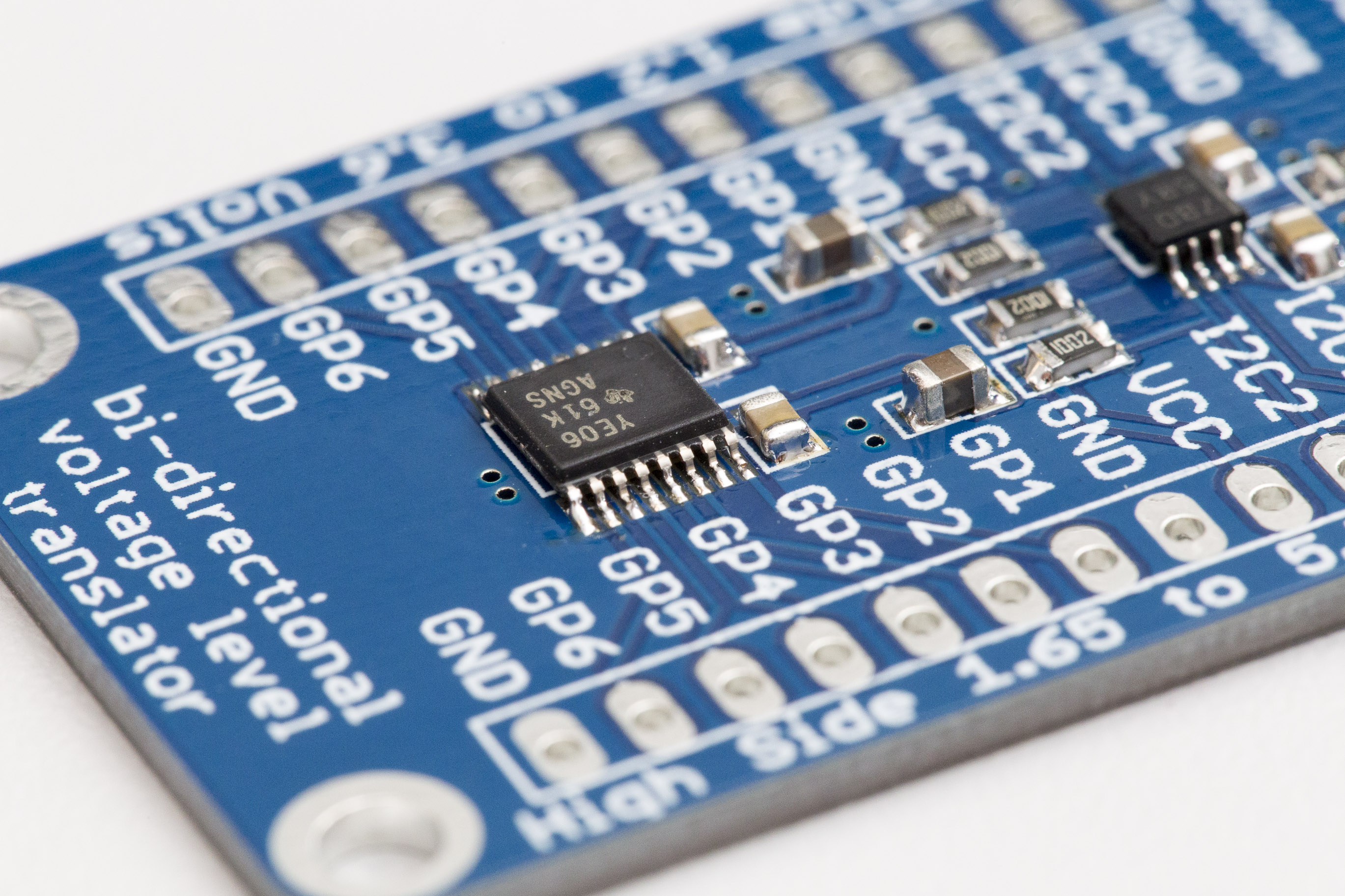
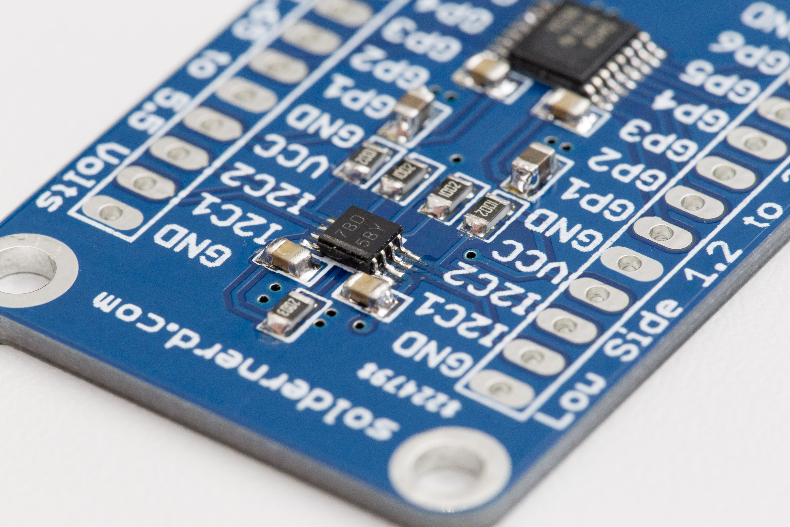
I ordered a few of these chips and laid out a simple board that contains the two chips together with the pull-up resistors and some decoupling caps. I also added two larger 10uF ceramic capacitors for a generous amount of bulk capacitance. The result is a tiny little board (45x30mm) that can universally be used to translate between almost any two logic voltages for almost any protocol.
Giving dirtypcbs.com a try
I can think of a lot of situations where it could be useful. But the main reason for this project was to gain some experience with getting a PCB professionally manufactured by a board house. For several years I have done my own designs but I always milled and drilled them myself. This had pros and cons. I never had to worry about silk screens or solder masks because my boards never had any. On the other hand I suffered from the lack of plated-through holes. Vias were always a pain in the arse because I had to manually solder in pieces of wire to connect the two sides. And it was very difficult if not impossible to put a via below a component which made the layout challenging when working with ICs with many and/or tightly spaced pins.
So this simple project seemed perfect to gain some experience in getting a design made by a board house. I chose dirtypcbs.com for their unbeatable prices and read their requirements and restrictions.

Here are some things to watch out for:
- If you’re working with Eagle you can download a design rule file to automatically check if your design fulfills their requirements. This is great for checking things like minimum via size or trace width/spacing.
- Make your own gerber files. Yes, you can just send dirtypcbs.com your Eagle files and they will take care of it. But I highly recommend you do it yourself so you know what you’re getting. It’s not difficult. Just download their .cam file and run it. I modified it somewhat so the file names reflect what the file contains. The file types themselves are rather cryptic.
- View the gerbers online: There are several online gerber viewers available for free. I particularly like the online viewer at mayhewlabs.com. Just drag and drop the gerber files produced in Eagle and get a beautiful 3D view of your design. Check it carefully to be sure the gerbers represent what you are after. My workflow was rather iterative: I produced the gerbers, looked at them online, changed something in Eagle, produced some new gerbers… Again and again until I was happy.
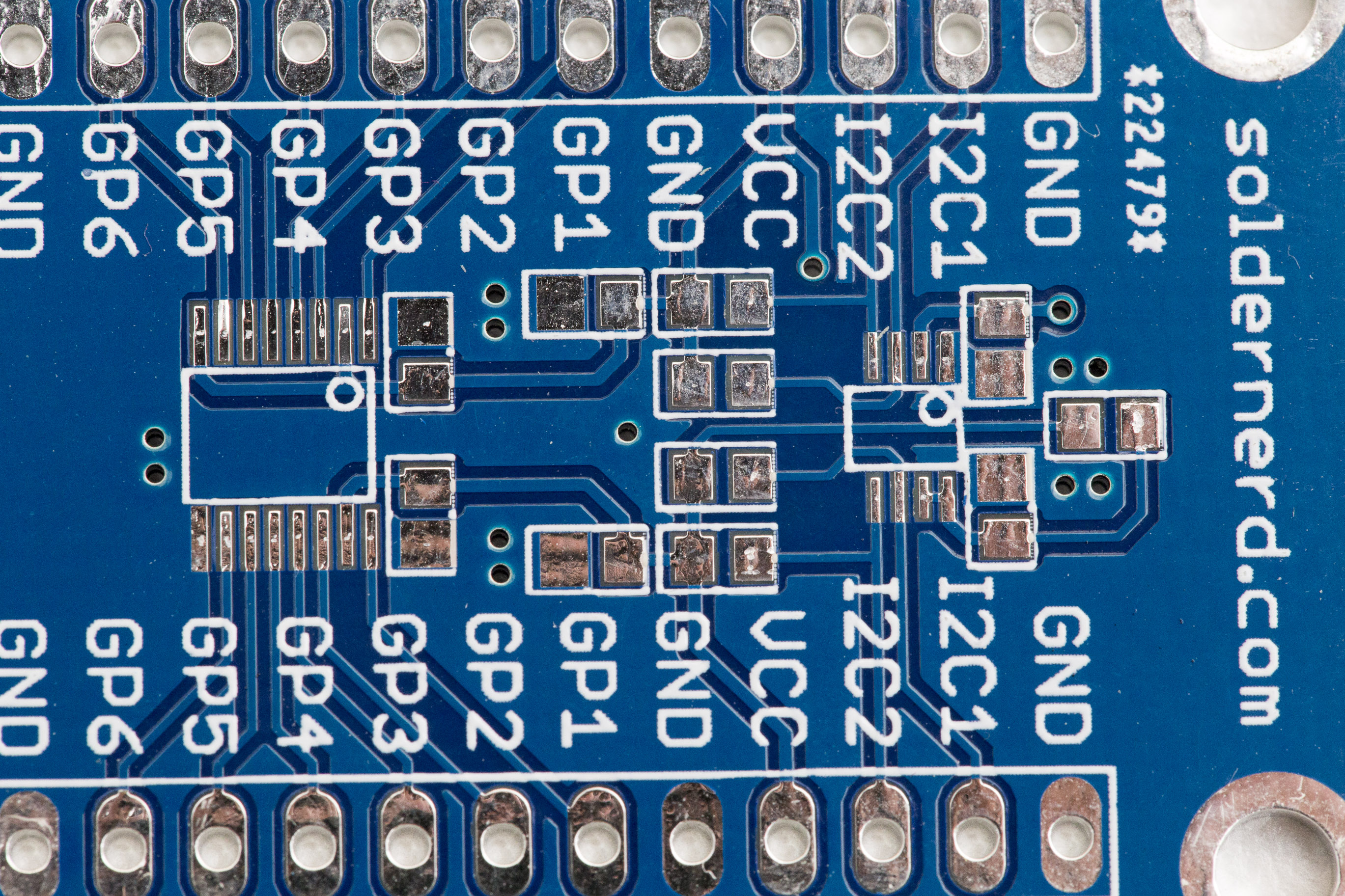
- Control what’s on your silk screen. A lot of the silk screen comes directly from the component libraries. Typically, the libraries print the outline, orientation, part name and part value on the silk screen. Unless your layout has a loooot of space between components the silk screen will soon be cluttered with all that information. I recommend you make your own libraries. You can then change the components to only contain the information you want and how you want it. I ended up only putting the outline and orientation of the components on the silk screen.
- Be aware that the design rule check will not look at your silk screen. You need to make sure your silk screen meets the minimum width of 0.15mm. If you’re using vector fonts (as you should) the math is simple. Just multiply the font size by the font ratio to calculate the line width. Example: A 70mils font size with a 10% ratio gives a line width of 7mils or 0.178mm.
- Make sure your silk screen doesn’t overlap any of the pads. Again, he design rule check will not check for this. The board house might avoid printing the silk screen over an exposed pad but I wouldn’t bet on it.
- Eagle seems to do quite a good job with the solder mask without any manual intervention but check the result carefully using the gerber viewer. Pay particular attention to the vias. You generally want your vias to be covered with solder stop – there’s no reason to have them exposed. But you might have some vias that you use as pads to access some signal for testing and debugging. Make sure they are not covered by the solder mask. An easy way to distinguish by the two types of vias is by drill size. You can set this parameter under DRC -> Mask -> Limit.

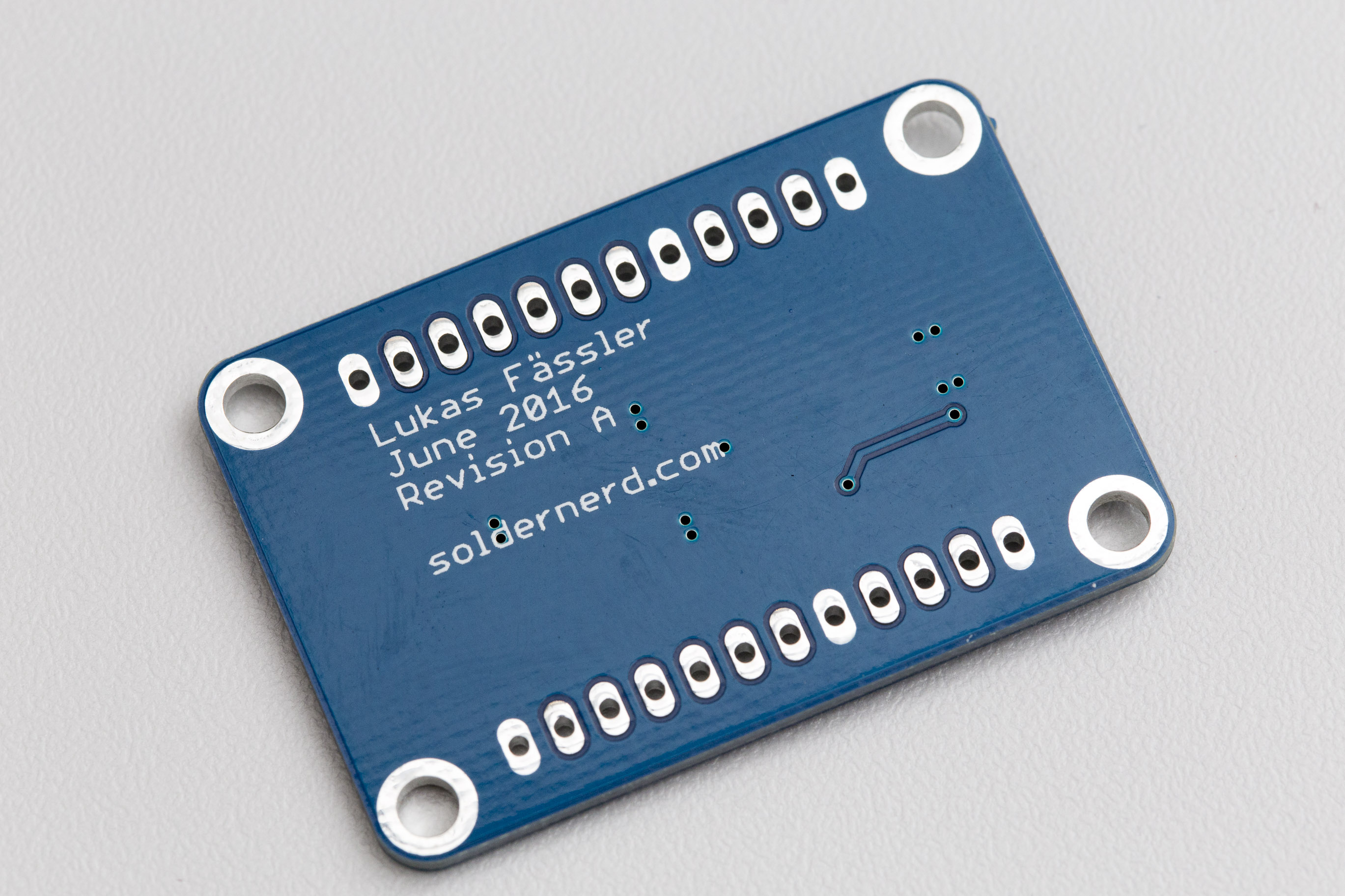
It took me quite some time until I had my files ready for manufacturing. Especially given the simple nature of this project. I then ordered a proto-pack from dirtypcbs.com. I went for a industry-standard 1.6mm (they default to 1.2mm) FR4 with a cool-looking (and non-standard) blue solder mask at no extra cost. Some 3 weeks later I found 10 of those nice little boards in my mailbox. They are quite precisely how I expected from the gerber viewer. When you look at them close enough you’ll notice that the solder mask and silk screen are not perfectly aligned. The silk screen could also be somewhat cleaner. But don’t get me wrong – I’m not complaining. The quality is absolutely ok, these are nice little boards. And at this price – I paid 14$ including everything – they are simply amazing. Thank you, dirtypcb.
So the board house test was a success but how about the rest? So far I’ve only populated a single board. And while I haven’t actually used it yet I have performed some tests with a signal generator and a scope.
PCA9306 for I2C
So let’s look at the PCA9306′ performance in some more detail.
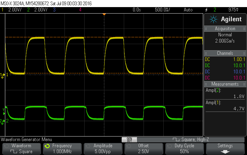
The chip performs excellently when translating from a high voltage to a lower voltage. In the example above it is translating from 5 volts to 1.8 volts at a very high 1MHz frequency and the wave forms still look nice.

Translating in the opposite direction (1.8 to 5 volts) everything is fine at 100kHz.
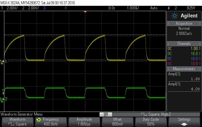
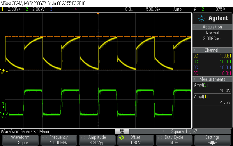
At 400kHz the output waveform starts to look very jagged, however.
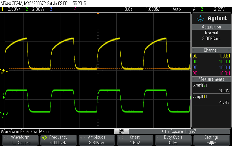
But of course, translating from 1.8 to 5 volts is a rather extreme example. In the much more likely scenario of translating from 3.3 to 5 volts the chip performs reasonably well, even at 400kHz. And I2C doesn’t usually happen at frequencies higher than that. An Arduino, for example, will usually work at 100kHz. So I’m very happy with the performance so far.
TXB0106 for SPI and the like
Now let’s look at the TXB0106.

Translating from 5V to 1.8V at a modest 100kHz is rather undemanding and the waveforms look nothing but perfect.
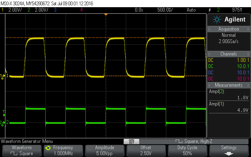
Even up at 1MHz this translation works totally fine.

Translating the opposite way, from 1.8V to 5V is more demanding but works very well at 100kHz.
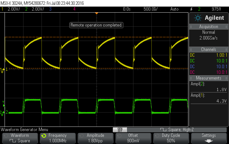
However, at 1Mhz the wave forms start to look pretty uggly. And with a protocol like SPI it is much more likely to actually operate at 1MHz. Note that the glitches might be an artefact of my primitive test setup.
As with the other chip, the output signal starts to better when only translating from 3.3 volts to 5 volts. As mentioned above this is a much more likely application and the chip does a decent job even at 1Mhz.
Support this blog – Buy one
By the way: If you need one of these universal voltage level translators you can support this blog by ordering one (fully assembled) for USD 20, including worldwide shipping. Just use the contact form on the about me page.
With the following link you can download the Eagle files as well as the gerbers. Just click here.


